BUK6D43-40P: Detailed Explanation of 40V P-Channel Automotive Grade MOSFET and Datasheet
Overview and Product Positioning
The
BUK6D43-40P is a 40V P-channel enhancement mode power MOSFET introduced
by Nexperia-USA-Inc. It utilizes advanced Trench MOSFET technology and is
housed in a compact DFN2020MD-6 (SOT1220) plastic package. As an
AEC-Q101 qualified automotive-grade component, it primarily targets
high-reliability application scenarios in automotive electronics and
industrial control.
This
MOSFET is particularly suitable for medium-to-low power switching
applications, such as relay driving, load switching, and various
switching circuits. Its maximum junction temperature of 175°C and the
miniaturized package design meet the dual demands of modern electronic
systems for high-temperature operation and miniaturization.
Structure and Operating Principle of BUK6D43-40P
The
BUK6D43-40P is a P-channel enhancement mode MOSFET. Its
high-performance semiconductor material gives it a very low on-state
resistance (Rds(on)) when conducting.
-
On-State: When the gate-to-source voltage (Vgs) reaches a certain threshold, a
conductive channel forms in the semiconductor material, allowing current
to flow between the source and drain. The MOSFET is in the on-state.
-
Off-State: When the gate-to-source voltage is below the gate threshold voltage,
the conductivity in the channel disappears, current between the source
and drain is cut off, and the MOSFET is in the off-state.
Features and Advantages of BUK6D43-40P
-
Low On-Resistance: The BUK6D43-40P operates with low resistance, making it especially
suitable for high-efficiency power converters. Its on-resistance Rds(on)
can be as low as 43 mΩ, effectively reducing energy loss and heat
generation.
-
High Current Handling Capability: With a maximum drain current of -14 A, it is suitable for higher power
applications, capable of handling various high-current loads and
providing stable performance.
-
High Thermal Stability: The operating junction temperature range of this MOSFET is from -55°C
to +175°C, allowing normal operation in extreme environments. This makes
it particularly suitable for industrial-grade, high-temperature
applications, or automotive electronics.
-
High Switching Speed: The BUK6D43-40P features fast switching characteristics, enabling quick
transitions between on and off states. This reduces energy loss during
switching and improves efficiency.
-
Low Switching Loss: Due to its excellent switching speed and on-resistance, the BUK6D43-40P
has low switching losses during switching operations, which is crucial
for high-efficiency power systems.
-
High Reliability: The structural design and materials used in this MOSFET ensure stable
performance even after numerous switching cycles, maintaining high
reliability under prolonged load.
Detailed Technical Parameters
For a more comprehensive understanding of the BUK6D43-40P's performance, here are its main technical parameters:
These
parameters show that the BUK6D43-40P maintains good conduction
characteristics at both 4.5V and 10V drive voltages, making it suitable
for different logic level interfaces, while its capacitance
characteristics optimize switching performance.
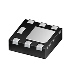
Package and Pin Information
The BUK6D43-40P uses the DFN2020MD-6 (SOT1220) package, a leadless, ultra-thin surface-mount package.
-
Dimensions: Only 2.0mm × 2.0mm × 0.65mm, greatly saving PCB space.
-
Features: The package has a thermal pad on the bottom, which effectively transfers heat generated by the chip to the PCB.
-
Process: Features a wettable flank design, allowing for Automated Optical
Inspection (AOI) after soldering, enhancing process reliability required
for automotive applications.
For
detailed pin layout and pad design of the DFN2020MD-6 package, refer to
the pinout and pad pattern diagrams provided in the product datasheet.

Application Areas of BUK6D43-40P
Due
to its high efficiency and reliability, the BUK6D43-40P is suitable for
various applications, particularly excelling in the following fields:
-
Switch Mode Power Supplies (SMPS): Widely used in various SMPS designs, it provides stable power
conversion efficiency under high-frequency, high-current conditions,
suitable for devices like battery chargers, computer power supplies, and
TV power supplies.
-
DC Motor Drive: This MOSFET can be used as a drive switch for DC motors, controlling
motor start/stop and speed variation, especially in robotics, automation
equipment, and power tools.
-
Load Switching and Power Protection: In load switch applications, the BUK6D43-40P is used in current control
and protection circuits, helping to improve the stability and safety of
the entire system.
-
Automotive Electronics: Due to its high-temperature tolerance and high-current characteristics,
it is also widely used in automotive electronic systems, such as
Battery Management Systems (BMS), electric vehicle drive control, and
onboard chargers.
-
High-Power Electronic Equipment: In electronic devices requiring high power, high efficiency, and high
reliability, the use of the BUK6D43-40P can effectively enhance device
performance and lifespan.
Usage Considerations
-
Polarity Attention: As a P-channel MOSFET, the voltage and current polarity are opposite to those of N-channel MOSFETs.
-
ESD Protection: MOSFETs are electrostatic sensitive devices; appropriate ESD protection measures must be taken during assembly and use.
-
Thermal Management: Although the package is small, good PCB thermal design must still be considered in high-current applications.
-
Drive Voltage: Ensure sufficient gate-source voltage (recommended -10V) is provided to achieve the lowest on-resistance.
BUK6D43-40P Datasheet PDF
Summary
The
BUK6D43-40P is a high-performance P-channel MOSFET. Leveraging its low
on-resistance, high current handling capability, wide operating
temperature range, and high switching speed, it plays a significant role
in various high-efficiency power and power electronic equipment.
Whether in switch-mode power supplies, DC motor drives, automotive
electronics, or load switching applications, this MOSFET delivers
excellent performance and reliability, making it a crucial component in
modern electronic devices.