Previous Chapter:BUK9K35-60E Detailed Introduction and Data sheet
Next Chapter:BUK9K17-60E Detailed Introduction and Datasheet
BUK9K29-100E Dual N-Channel MOSFET Explained: Ideal for High-Performance Automotive Electronics Applications
Post Date:2025-11-12
BUK9K29-100E Dual N-Channel MOSFET Explained: Ideal for High-Performance Automotive Electronics Applications
In automotive electronics and industrial control, efficient and reliable power switching devices are central to system design. Nexperia's BUK9K29-100E is a dual N-channel logic-level TrenchMOS FET designed for high-performance applications. With its superior electrical characteristics and robust package design, it is an ideal solution for various power switching applications in 12V automotive systems. This article will provide an in-depth analysis of the device's key features, technical parameters, and application scenarios.

1. Product Overview
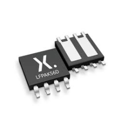
The BUK9K29-100E is a dual N-channel TrenchMOS logic-level FET manufactured by Nexperia, packaged in an LFPAK56D (dual Power-SO8) package.
This product complies with AEC-Q101 standards and is designed for demanding automotive electronic environments. Its rated junction temperature reaches 175°C, enabling it to withstand the high-temperature operating environments common in automotive applications.
This MOSFET integrates two high-performance N-channel transistors in a single package, providing a 100V drain-source voltage rating and 30A continuous drain current capability, enabling high power handling within a limited space.
2. Key Features and Benefits
2.1 Dual MOSFET Design
The BUK9K29-100E integrates two independent N-channel MOSFETs in a single package. This integrated design significantly saves board space, simplifies layout design, and improves system integration. For applications requiring multiple switching devices, such as half-bridge circuits and motor drive circuits, this dual MOSFET design significantly reduces component count and mounting complexity.
2.2 Logic-Level Gate Drive
As a true logic-level gate device, the BUK9K29-100E maintains a gate-source threshold voltage above 0.5V even at high temperatures of 175°C. This characteristic allows it to be directly driven by microcontrollers, DSPs, or logic chips without additional level shifting circuitry, simplifying design and reducing system costs.
2.3 Low On-Resistance
The BUK9K29-100E exhibits excellent conduction characteristics, with a maximum on-resistance of only 27mΩ at VGS = 10V. Even at a gate drive voltage of 5V, its on-resistance is only 29mΩ. Low on-resistance translates to lower conduction losses and higher system efficiency, a significant advantage particularly pronounced in high-current applications.
2.4 High Power Handling Capability
This device boasts a maximum power dissipation capability of 68W and can handle pulsed drain currents up to 118A, enabling it to withstand transient overloads and surge currents, thus enhancing system reliability and robustness.
2.5 Excellent Switching Characteristics
The BUK9K29-100E has a gate charge of only 54nC. This lower gate charge allows for faster switching speeds, simplifies drive circuit design, reduces switching losses, and improves efficiency in high-frequency applications.
3. Detailed Technical Specifications
Parameter Value Conditions
Drain-Source Voltage (VDSS) 100V Maximum
Continuous Drain Current (ID) 30A at 25°C
Pulse Drain Current (IDM) 118A -
Gate-Source Voltage (VGSS) ±10V Maximum
On-Resistance (RDS(on)) 27mΩ VGS=10V, ID=10A
On-Resistance (RDS(on)) 29mΩ VGS=5V
Gate-Source Threshold Voltage (VGS(th)) 2.1V ID=1mA
Total Gate Charge (Qg) 54nC VGS=10V
Input Capacitance (Ciss) 3491pF VDS=25V
Maximum Power Dissipation (PD) 68W -
Operating Junction Temperature (Tj) -55°C ~ +175°C -
Table: BUK9K29-100E Main Technical Specifications
4. Package and Pin Information
The BUK9K29-100E uses an LFPAK56D (SOT-1205) package, an 8-lead surface-mount package offering excellent thermal performance and power density. LFPAK packaging technology provides lower thermal resistance and higher reliability than traditional SO-8 packages while maintaining a similar footprint.
This package design allows for efficient heat transfer to the PCB through bottom-mounted heat dissipation, utilizing a copper layer as a heat sink, significantly improving power handling capabilities. With package dimensions of 4.7mm x 5.3mm x 1.05mm, it is ideal for space-constrained applications.
5. Application Areas
The BUK9K29-100E is designed for 12V automotive systems, and its applications include:
5.1 Automotive Electronics Applications
Motor Control: For motor drives in power windows, wipers, seat adjustments, etc.
Lighting Control: Headlights, fog lights, turn signals, and other lighting controls
Solenoid Control: Solenoid valve drives in transmissions and engine management systems
Transmission Control: Clutch and shift control in automatic transmissions
5.2 Industrial Applications
Stepper Motor Drive: Precision motor control in automated equipment
Power Management: DC-DC converters, power switching circuits
Industrial Automation: PLC output modules, machine control
6. Design Considerations and Precautions
6.1 Thermal Management
Although the BUK9K29-100E uses a thermally enhanced package, appropriate thermal management should still be considered in high-power applications. The design should ensure the following:
Provide sufficient copper area for heat dissipation
Consider using thermal vias to transfer heat to internal layers
Derating may be necessary in high-temperature environments
6.2 Driver Circuit Design
Although the BUK9K29-100E is a logic-level device, a sufficiently steep gate drive waveform is still required to minimize switching losses. Recommendations:
Use a dedicated gate driver chip
Optimize the gate resistor to balance switching speed and EMI
Add appropriate pull-down resistors between the gate and source to prevent accidental turn-on
6.3 Parallel Operation
For applications requiring higher current capability, consider using two switching units from a dual MOSFET in parallel. However, note the following:
Ensure both units operate within their safe operating areas
Consider potential current imbalances
Appropriate derating to improve reliability
7. Environmental Compliance and Reliability
The BUK9K29-100E complies with RoHS standards and does not contain restricted hazardous substances. As an automotive-grade product, it has passed the stringent AEC-Q101 certification, ensuring high reliability and long lifespan in harsh environments.
8.BUK9K29-100E Datasheet

9. Summary
The BUK9K29-100E dual N-channel logic-level MOSFET, with its high integration, excellent switching characteristics, low on-resistance, and robust package design, is an excellent solution for power switching applications in automotive electronics and industrial control. Its 100V withstand voltage and 30A current capability, combined with the convenience of logic-level drive, simplifies system design, increases power density, and ensures high reliability and efficiency.
Whether used in traditional automotive electrical systems or emerging industrial automation equipment, the BUK9K29-100E delivers performance that meets demanding requirements, making it an ideal choice for engineers designing high-performance power switching circuits.
Previous Chapter:BUK9K35-60E Detailed Introduction and Data sheet
Next Chapter:BUK9K17-60E Detailed Introduction and Datasheet