BUK9K35-60E Detailed Introduction and Data sheet
BUK9K35-60E Detailed Introduction and Data sheet
Overview

The BUK9K35-60E-115 is an N-channel logic level enhancement mode power MOSFET manufactured by NXP Semiconductors. It utilizes advanced Trench Field Stop technology, designed to provide extremely low on-state resistance, high switching speed, and excellent robustness.
It is an ideal choice for medium to high-power switching applications, particularly common in automotive and industrial fields.
BUK9K35-60E Detailed Introduction
I. Core Identity and Positioning
-
Model: BUK9K35-60E
-
Manufacturer: Infineon Technologies
-
Nature: An N-channel enhancement mode power MOSFET.
-
Technology: Utilizes Infineon's advanced Trench Field Stop technology.
-
Positioning: A balanced power switching device for industrial, consumer electronics, and automotive fields, offering a balance of low on-state resistance and high switching performance within the 600V voltage rating. Its logic level drive characteristics make it easy to use.
II. Key Characteristics and Absolute Maximum Ratings
These parameters define the operational limits of the device and must not be exceeded.
| Parameter | Symbol | Value | Condition/Explanation |
|---|---|---|---|
| Drain-Source Voltage | VDSS | 600 V | Defines the maximum voltage that can be sustained between drain and source. |
| Continuous Drain Current | ID | 18.5 A | At case temperature (Tc) = 25°C. |
|
|
|
11.8 A | At case temperature (Tc) = 100°C. This value is more critical for thermal design. |
| Gate-Source Voltage | VGS | ±20 V | The gate-source voltage must not exceed this range, otherwise permanent damage may occur. |
| Single Pulse Avalanche Energy | EAS | 460 mJ | An indicator of the ability to withstand accidental overvoltage (e.g., spikes from inductive loads). |
| Operating Junction Temperature | TJ | -55 to +150 °C | The temperature range of the silicon chip itself. |
| Storage Temperature | Tstg | -55 to +150 °C |
|
III. Core Electrical Parameters (@ Tj = 25°C unless otherwise specified)
These parameters describe the device's performance under normal operating conditions.
| Parameter | Symbol | Typical Value/Range | Condition | Importance |
|---|---|---|---|---|
| Gate Threshold Voltage | VGS(th) | 2.5 - 4.0 V | VDS=VGS, ID=250µA | Logic level compatible, can be directly driven by 3.3V/5V microcontrollers. |
| Static Drain-Source On-Resistance | RDS(on) | max. 0.35 Ω | VGS = 10 V, ID = 9.3 A | Core parameter. Determines power loss and heating during conduction. Lower is better. |
| Total Gate Charge | Qg | 28 nC (typ.) | VGS = 10 V | Key parameter for switching speed. Lower value means lower switching loss and easier driving. |
| Input Capacitance | Ciss | 1350 pF | VDS=400V, VGS=0V | Affects the current demand of the gate drive circuit. |
| Output Capacitance | Coss | 95 pF | VDS=400V, VGS=0V | Affects the voltage rise time during turn-off. |
| Reverse Transfer Capacitance | Crss | 14 pF | VDS=400V, VGS=0V | Causes the "Miller effect," a key capacitance during switching. |
IV. In-depth Interpretation of Technical Advantages
Field Stop Technology:
-
What it is: Based on traditional planar MOSFETs, a highly doped "field stop layer" is added to the drain region.
-
Benefit: This layer effectively blocks the electric field from penetrating into the substrate, allowing the silicon wafer to be made thinner for the same voltage rating.
-
Result: Significantly reduces on-state resistance (RDS(on)) while maintaining a high breakdown voltage (600V). This is the foundation of high efficiency.
Logic Level Drive:
-
Traditional MOSFETs often require 10V-15V VGS to fully turn on. The lower VGS(th) of the BUK9K35-60E means that only 5V or even 3.3V gate voltage is needed to achieve sufficient conduction.
-
Design Convenience: Engineers can directly use microcontroller GPIO pins to drive it, eliminating the need for complex gate driver ICs, simplifying the circuit and reducing cost.
Fast Switching Capability:
-
The lower gate charge (Qg) means the drive circuit requires less time to charge and discharge the gate capacitance.
-
Benefit: Fast switching speed and low loss during the switching transition (switching loss). This makes it very suitable for high-frequency switching applications like Switch-Mode Power Supplies (SMPS), allowing higher operating frequencies, thereby reducing the size of transformers and filters.
Ruggedness and Reliability:
-
High Avalanche Energy Capability (EAS): When inductive loads (like motors, transformers) are suddenly disconnected, they can generate spikes far exceeding the supply voltage. The EAS parameter indicates this device can absorb and dissipate a certain amount of accidental overvoltage energy without damage, improving system robustness.
-
AEC-Q101 Qualification: This is an automotive-grade reliability standard.
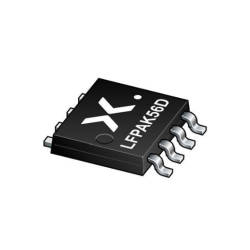
BUK9K35-60E Package and Pin Definition

Working Principle of BUK9K35-60E
Let's explain the working principle of the BUK9K35-60E in simple terms. We will start from its "role positioning" and gradually delve into its internal physical mechanisms and external control logic.
I. Core Role: A Voltage-Controlled High-Speed Electronic Switch
You can most simply understand the BUK9K35-60E as a voltage-controlled, single-pole, high-speed, contactless electronic switch.
-
Control Terminal (Gate G): Like the handle of a water tap. You don't need great force (current) to turn it, just provide the appropriate "water pressure" (voltage) to control the main water flow's on/off state.
-
Main Circuit Path (Drain D to Source S): Like the main path of the water pipe. When the handle (gate) is opened, water (current) can flow rapidly from the D terminal to the S terminal. The resistance of this path is extremely low (only 0.35Ω), resulting in low loss and less heat generation.
-
Advantage of "Contactless": Compared to mechanical relays, it has no physical contacts, so it does not generate sparks during switching, has an extremely long lifespan, and operates very fast (up to millions of times per second).
II. Detailed Working Principle: From "Closing the Door" to "Opening the Door"
Its operational physics are based on the "Field Effect" – using an electric field to control the conductivity of a semiconductor channel.
-
Cut-off State (OFF)
-
Condition: Voltage between Gate (G) and Source (S) VGS = 0V (or below the threshold voltage, e.g., < 2.5V).
-
Internal Situation:
-
In the P-type silicon substrate, a reverse-biased PN junction is inherently formed, acting like a natural "barrier" between D and S.
-
At this point, even if voltage (e.g., 600V) is applied between D and S, there is no effective conductive channel. This PN junction blocks the current.
-
The resistance between D and S is nearly infinite, equivalent to an open switch, current ID ≈ 0.
-
-
External Manifestation: The circuit is open, the load (e.g., motor) does not operate.
-
-
Saturation State (ON)
-
Condition: Apply a sufficiently high positive voltage VGS ≥ 10V between the Gate (G) and Source (S).
-
Internal Situation (Core of Field Effect):
-
This positive gate voltage creates a strong vertical electric field across the silicon oxide insulating layer below the gate.
-
This field acts like a magnet, attracting negatively charged electrons from the P-type substrate to the surface region directly under the gate.
-
When enough electrons are attracted, an N-type conductive channel forms on the surface of the originally P-type region, connecting the two N+ regions (source and drain).
-
This channel acts like a "bridge," breaking the barrier of the previous PN junction.
-
-
External Manifestation: A very low-resistance (0.35Ω) conductive path is established between D and S, allowing current ID to flow smoothly from the D terminal to the S terminal. Equivalent to a closed switch, the load starts working.
-
III. Key Operational Characteristics in Circuit Design
-
Logic Level Drive:
-
The BUK9K35-60E has a low gate threshold voltage (approx. 2.5V-4V), meaning only 5V or even 3.3V is needed to initiate the formation of the conductive channel. To achieve full conduction (lowest RDS(on)), 10V is typically recommended. But even with only 5V, it can conduct well, allowing microcontrollers to control it directly.
-
-
Fast Switching and Gate Charge (Qg):
-
The switching process is essentially the charging and discharging of the gate capacitance.
-
Turn-On: The drive circuit needs to quickly charge the gate capacitance, raising VGS from 0V to the turn-on voltage. The BUK9K35-60E's low Qg (28nC) means charging is fast, leading to rapid switching.
-
Turn-Off: The drive circuit needs to quickly discharge the gate capacitance to 0V.
-
Design Implication: Your microcontroller or driver IC must be able to provide sufficient instantaneous current to charge and discharge this capacitance quickly; otherwise, the switching process slows down, causing switching losses to increase dramatically and the device to overheat severely.
-
-
Body Diode (Parasitic Diode):
-
In the MOSFET's structure, a parasitic diode formed by the P-body and N- drift region is inherently created, connected in reverse parallel between D and S.
-
Function: This diode is crucial in certain circuits (e.g., motor drives, relay drives). It provides a path for the reverse induced electromotive force (back EMF) generated when an inductive load is switched off, protecting the MOSFET itself from high-voltage breakdown.
-
Note: This diode typically has a slow recovery speed and is not suitable for use as a freewheeling diode in high-frequency switching circuits; an external fast recovery diode is needed in such cases.
-
IV. Summary of Working Process
In a typical PWM motor control circuit, the BUK9K35-60E operates as follows:
-
MCU Issues Command: The microcontroller outputs a 3.3V/5V PWM square wave signal from its I/O pin.
-
Gate Voltage Establishment: This signal is applied directly (or through a small series resistor) to the MOSFET's gate (G), charging the gate capacitance. VGS rises rapidly.
-
Channel Formation & Conduction: When VGS exceeds the threshold voltage, the N-type conductive channel forms, and the MOSFET turns on. Current flows from the positive power supply, through the motor, into the D terminal, and out the S terminal back to the negative supply. The motor receives power.
-
PWM Turn-Off: The MCU outputs a low level (0V). The gate capacitance discharges rapidly through the drive circuit, and VGS drops to 0V.
-
Channel Disappearance & Cut-off: The conductive channel disappears, the MOSFET turns off, current is cut off, and the motor stops receiving power.
-
Handling Back EMF: At the moment of turn-off, the motor's inductance generates a reverse EMF. The body diode then conducts, clamping this spike energy and returning it to the power supply, protecting the MOSFET's D-S junction from overvoltage breakdown.
-
High-Speed Repetition: The above process repeats at a very high frequency (e.g., 20kHz). By adjusting the PWM duty cycle (the proportion of high-level time), the average voltage to the motor is controlled, thereby achieving speed regulation.
In summary, the working principle of the BUK9K35-60E involves using the voltage signal applied between the gate and source to create or eliminate a conductive channel within its internal semiconductor, thereby acting like an invisible hand to control the on/off state of the main power circuit with high speed and precision.
BUK9K35-60E Technical Advantages: Why Choose It?
-
Field Stop Technology: The Foundation of Performance
-
Traditional planar MOSFETs struggle to balance low resistance with high voltage ratings. Field Stop technology adds a highly doped layer inside the chip that effectively cuts off the electric field, allowing the silicon wafer to be thinner while maintaining high voltage resistance. This directly results in low on-state resistance (RDS(on)) and smaller chip area, achieving high efficiency and low cost.
-
-
Ease of Use: Simplifies Design
-
The "Logic Level" drive characteristic is one of its main selling points. Engineers no longer need to design complex gate drive circuits with 12V-15V outputs for driving high-voltage MOSFETs; they can use the MCU's I/O pins directly, simplifying PCB layout and reducing BOM cost and design complexity.
-
-
Born for High Frequency: Increases Power Density
-
Low Qg and Ciss result in very short switching transition times. This is crucial for high-frequency Switch-Mode Power Supplies (SMPS) because higher switching frequencies allow the use of smaller, lighter transformers, inductors, and capacitors, thereby achieving higher power density (smaller size for the same power).
-
-
Automotive Grade Quality: Assurance of Reliability
-
AEC-Q101 qualification is not achieved overnight. It means the BUK9K35-60E has undergone a series of extreme tests including temperature cycling, High Temperature Reverse Bias (HTRB), and highly accelerated stress testing (HAST). Choosing it is not just selecting a component; it's adding an insurance policy for the product's long-term stability and durability.
-
BUK9K35-60E Typical Application Scenarios
-
Switch Mode Power Supplies: As the main switch following the PWM controller, used in server power supplies, industrial power supplies, chargers, etc.
-
Motor Drives and Motion Control: Drives brushed/brushless DC motors in H-bridges or three-phase inverters, widely used in power tools, home appliances, and industrial robots.
-
Automotive Electronics: Used in engine management (injectors, ignition coils), body control (power windows, seats, LED lighting), and auxiliary power supplies for new energy vehicles.
-
Photovoltaic Inverters: Acts as a power switching element in the DC-AC conversion stage.
-
Uninterruptible Power Supplies: Participates in power conversion and backup control.
BUK9K35-60E Data sheet
 BUK9K35-60E-115.pdf
Summary
The BUK9K35-60E, manufactured by NXP, is a market-proven, well-balanced, and highly reliable power switching solution. It perfectly combines high voltage capability, low loss, ease of drive, and high ruggedness, making it a "go-to choice" for engineers facing medium to high-power switching applications. Whether for improving energy efficiency, reducing size, or ensuring stable operation in harsh environments, the BUK9K35-60E demonstrates its value as a classic power MOSFET.