C1815 Transistor Pinout, Equivalent, Datasheet & Circuit Diagram
What is the C1815 Transistor?
The C1815 transistor is a popular NPN transistor widely used in various electronic applications due to its compact size and excellent performance in low-power circuits. As a small-signal transistor, the C1815 is designed to handle relatively low current and voltage, making it a go-to choice for small signal amplification, switching, and other applications where efficiency is key. Although relatively inexpensive, the C1815 offers a robust set of features that make it indispensable in a wide range of consumer electronics, such as radios, audio devices, and even toys.

The C1815 is part of a family of small-signal transistors that have been widely used for decades. It is known for its efficiency and reliability in tasks like amplifying weak electrical signals or acting as a switch in circuits. Its TO-92 package makes it easy to handle and mount on circuit boards, which is one reason it has become a standard choice for many electronics designers and hobbyists.
What is the Voltage of a C1815 Transistor?
The voltage rating of a transistor is crucial because it determines how much voltage the component can safely handle before it is at risk of failure. The C1815 transistor has a maximum collector-emitter voltage (Vce) of 50V. This makes it suitable for circuits where moderate voltage levels are used, but not ideal for high-voltage applications. It is perfect for small-signal circuits, such as low-power audio amplifiers, radio frequency circuits, and switching circuits where voltage is relatively low.
The base-emitter voltage (Vbe) of the C1815 is typically around 0.7V. This is a standard voltage value for NPN transistors and represents the forward voltage drop across the base-emitter junction when the transistor is turned on. For the C1815, this value is optimal for most low-power electronic circuits, and it is consistent with the transistor's design specifications.
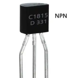
C1815 Transistor Pinout
The pinout of a transistor defines the arrangement of its terminals (or pins) and is critical for ensuring that the transistor is wired correctly in a circuit. The C1815 transistor is housed in a TO-92 package, which has three pins: Collector (C), Base (B), and Emitter (E).

Pin 1 (Emitter) – This is the pin through which the current exits the transistor. It is typically connected to ground in most circuits.
Pin 2 (Base) – The base pin controls the operation of the transistor. When a small current is applied to the base, it allows a larger current to flow from the collector to the emitter. The base is usually connected to a resistor to limit the current entering the transistor.
Pin 3 (Collector) – The collector pin is where the current enters the transistor. It is connected to the load or other circuit components through which the amplified signal or current flows.
C1815 Transistor Marking Diagram

C1815 Transistor Amplifier Circuit Diagram
The C1815 transistor amplifier circuit is a common application of the C1815 used to amplify weak electrical signals. These amplifiers are widely used in audio processing, signal conditioning, and even in radio receivers. In a basic C1815 transistor amplifier, the transistor works by taking an input signal and boosting its strength. The circuit typically includes a few key components:

A resistor at the base to limit the current that flows into the base.
A coupling capacitor at the input to block any DC bias and pass the AC signal.
A collector resistor to provide a load for the transistor, helping to develop the output signal.
An output capacitor to pass the amplified signal to the next stage while blocking DC voltage.
In this circuit, the input signal is applied to the base, and a biasing resistor ensures that the transistor operates in its active region. The amplified version of the signal appears at the collector, and a capacitor is used to isolate the amplified signal from the DC biasing components. This simple amplifier circuit can be used for audio preamps, signal processing, or radio frequency amplification.
What is the Function of the C1815 Transistor Amplifier?
The main function of the C1815 transistor amplifier is to take a weak input signal and increase its power or amplitude. This is crucial for applications like audio amplification or signal boosting, where the original signal is too weak to drive other components or produce usable output.
An amplifier circuit works by exploiting the transistor’s ability to modulate the current flowing from the collector to the emitter. When a small signal is applied to the base, it controls the larger current flowing through the collector-emitter path. This allows the transistor to amplify the signal, and the resulting output signal at the collector will have higher amplitude than the original input.
In audio applications, the C1815 can be used as part of a pre-amplifier circuit to boost weak audio signals before sending them to the power amplifier. Similarly, in radio circuits, it is used to amplify radio frequency signals, making them strong enough for further processing or transmission.
C1815 Transistor Features
Type: NPN
Maximum Collector-Emitter Voltage: 50V
Maximum Collector-Base Voltage: 50V
Maximum Emitter-Base Voltage: 5V
Maximum Collector Current: 150mA
Power Dissipation (Ptot): 300mW (0.3W)
Current Gain (hFE): 110 to 800
Base-Emitter Voltage (Vbe): 0.6V to 0.7V
Transition Frequency (ft): 250 MHz
Package Type: TO-92
Operating Junction Temperature: -55°C to +150°C
Storage Temperature: -55°C to +150°C
What are C1815 Transistors Used For?
The C1815 transistor is used in a variety of applications, ranging from basic signal amplification to more complex signal processing circuits. Some common uses include:
- Signal Amplification: The C1815 is frequently used in audio amplifiers, where it boosts weak audio signals for processing or driving speakers.
- Switching: Like most NPN transistors, the C1815 can be used as a switch in digital circuits, where it controls the flow of current through a load based on the input signal at the base.
- Oscillator Circuits: The transistor is commonly found in oscillators that generate periodic signals, such as square waves, used in timing circuits, clocks, and frequency generators.
- Radio Frequency Circuits: The C1815 is often used in radio receivers and other RF circuits due to its ability to amplify weak RF signals.
- Low-Power Electronics: Its low current consumption makes it very suitable for battery-powered devices, such as toys, portable radios, and small consumer electronics.
What is the Difference Between C1815 and 2N2222?
The C1815 and 2N2222 are both NPN transistors, but they have distinct characteristics that make them better suited for different types of applications. Let's compare the two in more detail:
|
Feature |
C1815 |
2N2222 |
|
Maximum Collector-Emitter Voltage |
50V |
40V |
|
Maximum Collector Current |
150mA |
800mA |
|
Current Gain (hFE) |
110 to 800 |
100 to 300 |
|
Base-Emitter Voltage (Vbe) |
0.6V to 0.7V |
0.7V to 1V |
|
Transition Frequency (ft) |
250 MHz |
250 MHz |
|
Package Type |
TO-92 |
TO-92 |
|
Power Dissipation (Ptot) |
300mW (0.3W) |
500mW (0.5W) |
C1815 Transistor Equivalent
If you're unable to find the C1815 transistor, several equivalent transistors can be used in its place. These transistors are similar in terms of specifications such as voltage, current, and current gain, making them suitable substitutes in most circuits. Here are some common equivalents for the C1815 transistor:
2N3904
Type: NPN
Voltage Rating: 40V
Current Rating: 200mA
Current Gain (hFE): 100-300
Package: TO-92
Application: Small-signal amplification, switching, and low-power circuits.
BC547
Type: NPN
Voltage Rating: 45V
Current Rating: 100mA
Current Gain (hFE): 110-800
Package: TO-92
Application: Small-signal amplification, low-noise audio circuits, and switching applications.
S8050
Type: NPN
Voltage Rating: 40V
Current Rating: 1A
Current Gain (hFE): 110-800
Package: TO-92
Application: Low-power amplifiers, general-purpose switching, and signal amplification.
2N2222
Type: NPN
Voltage Rating: 40V
Current Rating: 800mA
Current Gain (hFE): 110-800
Package: TO-92
Application: Switching, low-power amplification, and general-purpose applications.
2N5088
Type: NPN
Voltage Rating: 30V
Current Rating: 100mA
Current Gain (hFE): 200-800
Package: TO-92
Application: Audio amplifiers, low-noise applications, and signal amplification.
A1015
Type: NPN
Voltage Rating: 50V
Current Rating: 150mA
Current Gain (hFE): 200-800
Package: TO-92
Application: Low-power amplification, switching, and signal processing.
Each of these transistors has similar voltage and current ratings to the C1815 and can be substituted in most circuits, but always ensure that the specific characteristics of the replacement match your design requirements.
How to Test a C1815 Transistor?
Testing a C1815 transistor ensures it is functioning properly before integrating it into your circuit. Here’s a step-by-step guide on how to test the transistor using a multimeter in diode test mode:
1. Set the Multimeter to Diode Mode
First, set your multimeter to diode test mode. This mode is used to check for forward voltage drop across the transistor’s junctions, which is necessary for testing its functionality. Most digital multimeters have a diode test function, which is typically indicated by a diode symbol on the dial.
2. Identify the Transistor Leads
The C1815 is a 3-pin NPN transistor. To correctly test it, identify the following pins:
Pin 1 (Emitter): This is the leftmost pin when facing the flat side of the transistor.
Pin 2 (Base): This is the middle pin.
Pin 3 (Collector): This is the rightmost pin.
3. Test the Base-Emitter Junction
Place the positive probe of the multimeter on the base (Pin 2) and the negative probe on the emitter (Pin 1). A healthy C1815 will show a forward voltage drop of around 0.6V to 0.7V. This indicates that the base-emitter junction is functional and that the transistor can turn on. If the reading is much higher or there is no voltage reading at all, the transistor may be faulty.
4. Test the Base-Collector Junction
Next, place the positive probe on the base (Pin 2) and the negative probe on the collector (Pin 3). You should see a similar forward voltage drop of 0.6V to 0.7V, indicating the proper functioning of the base-collector junction. If there is no voltage drop or it’s too high, this suggests an issue with the junction.
5. Test the Collector-Emitter Junction
To check the collector-emitter junction, place the positive probe on the collector (Pin 3) and the negative probe on the emitter (Pin 1). The multimeter should show infinite resistance or no continuity, indicating that the transistor is off and the junction is non-conductive when the transistor is not active. If there is continuity, the transistor may be shorted.
6. Test the Emitter-Collector Junction
For completeness, reverse the probe positions: place the positive probe on the emitter (Pin 1) and the negative probe on the collector (Pin 3). The multimeter should show no continuity. If the reading shows continuity, the transistor is likely faulty or shorted.
7. Check for Shorts
Ensure that there is no short between any of the three pins—base, collector, and emitter. A shorted transistor will not function as expected in a circuit. The multimeter should show infinite resistance for all combinations of the transistor's leads when no current is flowing.
C1815 Transistor Datasheet
If you want to get more information about C1815 transistor, please click here to download C1815 Transistor Datasheet
Statement: All articles (images, texts, audio) on this site are uploaded and shared by users, or integrated from relevant internet sources, only for user's learning. If your rights are violated, please contact the administrator to delete! Link to this article: https://www.jinftry.com