Previous Chapter:What is diode?
Next Chapter:What is a thyristor and what are its advantages?
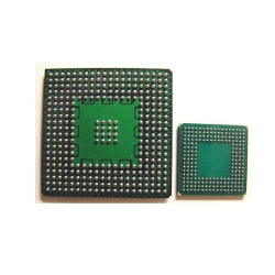
What is BGA
Post Date:2024-05-30,Intel
What is BGA
The full name of BGA is called "ball grid array", or "ball grid source array package". BGA can be an extreme product of LGA, PGA, or it can be arbitrarily replaced with different characteristics.Once the BGA is packaged, it is impossible for ordinary players to disassemble and replace it in a normal way unless it is through a professional instrument, but because it is done at once, the BGA can be made shorter and smaller.
Spherical contact display, one of the surface mount type packages. A spherical convex point is made on the back of the printed substrate according to the display mode to replace the pin, and the LSI chip is assembled on the front of the printed substrate, and then sealed with molded resin or potting method. Also known as raised point display carrier (PAC). Pin can be more than 200, is a multi-pin LSI for a package. The package body can also be made smaller than the QFP(four-side pin flat package). For example, a 360 pin BGA with a pin center distance of 1.5mm is only 31mm square; The QFP of pin 304 with a pin center distance of 0.5mm is 40mm square. And BGA doesn't have to worry about pin distortion like QFP. The package was developed by Motorola in the United States and was first adopted in devices such as portable phones and is likely to be popularized in personal computers in the United States in the future. Initially, the BGA had a pin (raised) center distance of 1.5mm and a pin number of 225. There are also some LSI manufacturers now developing 500-pin BGA. The problem with BGA is the appearance inspection after reflow soldering. It is not clear whether the appearance inspection method is effective. Some believe that due to the large center distance of the welding, the connection can be regarded as stable and can only be handled by functional inspection. The American Motorola company calls the package sealed with molded resin OMPAC, and the package sealed by potting method GPAC(see OMPAC and GPAC).

What are the advantages of BGA
Package efficiency: By reducing the package area, BGA enables a single chip to accommodate more pins, thus achieving a significant expansion of functionality.Easy assembly: Thanks to the ball design, the BGA can be self-centered during assembly, making the process of tinning smoother.
Enhanced reliability: Precision structural design and electrical performance optimization ensure high reliability of BGA.
Cost-effectiveness: BGA's optimized design not only improves performance, but also reduces overall costs.

BGA encapsulation definition
The Ball Grid Array (BGA) package is an array made at the bottom of the package substrate, and the solder ball is connected to the printed circuit board (PCB) as the I/O end of the circuit. The device packaged by the technique is a surface mount device.BGA(Ball Grid Array), referred to as BGA, translated as spherical contact array package, can also be translated as "ball grid array" or "network welding ball array" and "spherical array" and so on. It is a spherical contact made on the back of the substrate in an array way as a pin, and the LSI assembled on the front of the substrate (part of the BGA chip and the lead end are on the same side of the substrate) is a surface mount package for multi-pin LSI.
Compared with traditional foot mounted devices, BGA packaged devices have the following characteristics:
(1) High yield. By using BGA, the failure rate of 200x10-6 solder joints with fine spacing QFP can be reduced to two orders of magnitude without major changes to the process.
(2) Simple equipment. The center distance of the BGA solder joint is generally 1.27mm, which can be used by existing SMT process equipment. If the pin center distance of QFP is as small as 0.3mm, the pin distance is only 0.15mm, which requires very precise placement equipment and completely different welding processes, and it is extremely difficult to achieve.
(3) Large number of pins. The ratio of device extraction number to body size is improved. For example, a BGA with a side length of 31mm has 400 pins when the pitch is 1.5mm; When the spacing is 1mm, there are 900 pins. In contrast, a QFP with a side length of 32mm and a pin spacing of 0.5mm has only 208 pins.
(4) Small coplanar damage. Coplanar problems are significantly improved and coplanar damage is reduced.
(5) Pin firmly. The BGA pin is firm and does not have the problem of pin deformation like the QFP.
(6) Good electrical performance. The BGA pin is very short, making the signal path short, reducing the inductance and capacitance of the lead, and enhancing the electrical performance.
(7) Good heat dissipation. Spherical contact arrays facilitate heat dissipation.
(8) High packaging density. BGA is suitable for MCM packaging and is beneficial to achieve high density and high performance of MCM.

Classification of BGA packages
PBGA-- the English name is Plasric BGA, the carrier is a common printed board substrate, generally 2~4 layers of organic material composed of multi-layer board, the chip is connected to the upper surface of the carrier by wire press welding, plastic molding carrier surface connected with eutectic solder ball array.CBGA-- English name for CeramicBGA, the carrier is multi-layer ceramic, chip and ceramic carrier connection can have two forms: wire welding; Flip chip technology. It has the advantages of excellent electrical and thermal properties and good sealing.
CCGA- CCGA is another form of CBGA larger than 32*32mm, the difference is that the solder column is used instead of the solder ball. The solder column is connected by eutectic solder or fixed on the ceramic bottom by direct pouring.
TBGA-- The carrier adopts bimetal layer strip, and the chip connection adopts flip technology. Lighter and smaller packages can be achieved; Suitable for IO number can be more packaging; Have good electrical properties; Suitable for mass electronic assembly; High reliability of solder joints
Previous Chapter:What is diode?
Next Chapter:What is a thyristor and what are its advantages?