What is the TL494 Chip? Working Principle and Typical Circuit Diagram?

What is TL494?
TL494 is a fixed-frequency PWM circuit that includes all necessary functions for switch-mode power supply control, widely used in single-ended forward, half-bridge, and full-bridge switch-mode power supplies. The device integrates all functions required to construct a pulse-width modulation (PWM) control circuit on a single chip, primarily designed for power supply control, allowing flexible customization for specific applications.
TL494 Pin Descriptions and Functions
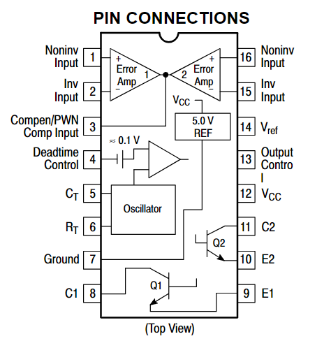
The TL494 has 16 pins, each serving specific functions such as error amplifier inputs, compensation/PWM comparator input, dead-time control, oscillator timing, ground, output collector and emitter, power supply, output control, and voltage reference. You can see the detailed diagram of typical TL494 chips and its functions as below:
(Diagram of TL494)
1. Non-Inverting Input: Error amplifier 1 non-inverting input.
2. Inverting Input: Error amplifier 1 inverting input.
3. Compensation/PWM Comparator Input: Connected to an RC network for stability.4. Dead-Time Control: Controls duty cycle from 0-45% with 0-4VDC input, also used for soft-start.
5. CT: External timing resistor for the oscillator.
6. RT: External timing capacitor for the oscillator. Frequency: f=1/RTCT.
7. GND: Ground.
8. Q1: Output 1 collector.
9. E1: Output 1 emitter.10. E2: Output 2 emitter.
11. C2: Output 2 collector.
12. Vcc: Positive power supply. 7-40VDC.
13. Output Control: Controls output mode. Ground for synchronized outputs, high for alternate outputs.
14. VREF: 5VDC reference voltage output.
15. Inverting Input: Error amplifier 2 inverting input.
16. Non-Inverting Input: Error amplifier 2 non-inverting input.
What are the main features of TL494?
the TL494 is a versatile PWM control circuit widely used in power supply designs due to its flexibility, reliability, and comprehensive feature set. Here are its key features:
- Two complete PWM control circuits can generate adjustable pulse-width modulation signals that control the switching of power transistors.
- Two error amplifiers, one for feedback control, one for overcurrent protection, enabling regulation of the output voltage or current.
- 5VDC reference power supply.
- Adjustable dead-time control between the switching of complementary power transistors, preventing shoot-through current in push-pull configurations.
- Output stage current up to 500mA.
- Output control for push-pull, half-bridge, or single-ended control, and dual output control allowing for independent control of two separate power stages or for use in push-pull configurations.
- Undervoltage lockout feature.
What is the Internal Structure of TL494?
TL494 is a fixed-frequency PWM circuit with an internal linear sawtooth oscillator. The frequency is adjustable with external resistors and capacitors. The pulse width of the output is determined by comparing the sawtooth waveform with two control signals. Power output transistors Q1 and Q2 are controlled by NOR gates. The pulse width decreases as the control signal increases. Here is a representative diagram of a TL494 chip.
(Representative block diagram of TL494)
Reference Regulator
The TL494 chip has a built-in reference source based on the bandgap principle, and the stable output voltage of the reference source is 5V, provided that the VCC voltage is above 7V and the error is within 100mV. The output pin of the reference source is pin 14 REF.
Oscillator
From the diagram, you can see a sawtooth oscillator in the internal of TL494, it produces sawtooth waves of 0.3 to 3V. The oscillation frequency can be adjusted by an external resistor Rt and a capacitor Ct, whose oscillation frequency is: f=1/RtCt, where Rt is in ohms and Ct is in farads. The sawtooth wave can be measured on the Ct pin.
Operational Amplifier
The TL494 integrates two single-supply operational amplifiers. The transfer function of the operational amplifier is ft(ni,inv)=A(NI-INV), but the output swing cannot be exceeded. In the general power supply circuit, the operation amplifier is connected to the closed-loop operation. Open loop is used in a few special cases, which is determined by the external input signal. The output of the two op-amps is connected to a diode, which is connected to the COMP pin and the post-stage circuit (comparator). This ensures that the higher output of the two op amps goes into the back-end circuit.
PWM Comparators
The output signal of the op amp (COMP pin) enters the positive input of the comparator inside the chip and compares the sawtooth wave into the negative input. When the sawtooth wave is higher than the signal of the COMP pin, the comparator outputs 0, otherwise it outputs 1.
The pulse trigger is on at the falling edge of the sawtooth wave and the comparator output 1, which interferes with the pulse trigger through a comparator to limit the maximum duty cycle. The maximum duty cycle per end can be set up to 45%, and the maximum duty cycle is about 42% when the operating frequency is above 150kHz (when the DTC pin level is set to 0).
The Working principle of TL494
The TL494 is a fixed frequency pulse width modulation circuit with a built-in linear sawtooth oscillator, the oscillation frequency can be adjusted by an external resistor and a capacitor, the oscillation frequency is as follows:
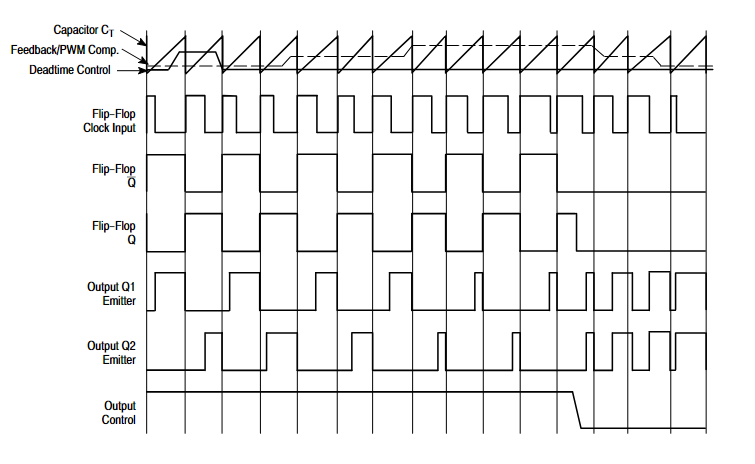
The width of the output pulse is achieved by comparing the positive sawtooth voltage on the capacitor CT. with the other two control signals. The power output tubes Q1 and Q2 are controlled by the OR not gate. The bistable flip-flop is stroked only when the clock signal is low, that is, only when the sawtooth voltage is greater than the control signal. As the control signal increases, the width of the output pulse will decrease. See the figure below.

The pulse-width modulation comparator provides a means for the error amplifier to adjust the output pulse width: when the feedback voltage changes from 0.5V to 3.5, the output pulse width drops from the maximum on-percentage time determined by the dead zone to zero. The two error amplifiers have a common-mode input range from -0.3V to (Vcc 2.0), which may be perceived from the output voltage and current of the power supply. The output of the error amplifier is usually flat, and it performs "or" operations with the inverting input of the pulse width modulator. It is this circuit structure that the amplifier needs only the smallest output to dominate the control loop.
When the comparator CT is discharged, a positive pulse appears on the output of the dead-time comparator, and the pulse-constrained bistable trigger timing, while stopping the output tubes Q1 and Q2. If the output control is connected to a reference voltage source, the modulated pulses are alternately output to the two output transistors at an output frequency equal to half that of the pulse oscillator. If operating in a single-ended state, and the maximum duty cycle is less than 50%, the output drive signal is obtained from the transistor Q1 or Q2, respectively. The output transformer has a feedback winding and the diode provides the feedback voltage. In single-ended operation mode, when higher drive current output is required, Q1 and Q2 can also be used in parallel, at this time, the output mode control pin needs to be grounded to close the bistable trigger. In this state, the output pulse frequency will equal the frequency of the oscillator.
Typical Circuits of TL494
There are two typical circuit designs by using TL494, one is smooth speed control and another is single-loop controller.Brushed Motor Smooth Speed Control
The PWM regulation of TL494 peripheral circuit is realized by TL494CN chip, and the main power device adopts the mode of parallel MOSFETs and multiple diodes. In order to realize smooth speed regulation of DC brush motor, pin 13 of TL494 is grounded to make TL494 work in single-end output mode and realize PWM duty cycle from 0 to 96% continuously adjustable.
Single-Loop Controller
The single-loop controller utilizes the TL494’s error amplifier and PWM functions, converting the PWM signal to a variable DC voltage for precise control, the working principle including input circuit, PWM circuit, output circuit and operation.
a) Input Circuit
Two operational amplifiers (IC1A, IC1B) form active simple second-order low-pass filters for feedback and set-point signals. Symmetrical design, cutoff frequency fp=4Hz, C1 and C2=1μF, R1 and R2=16kΩ.
b) PWM Circuit
Uses TL494's error amplifier I, with IN+(16) grounded and IN-(15) high. Protection via R13 and R10 voltage division, 4 pin at ~0.3V.
c) Output Circuit
Converts PWM to DC voltage through rectification and filtering. R15 as load, C8 voltage proportional to TL494 pulse width.
d) Operation
When feedback signal > set value, TL494 reduces pulse width, lowering control signal voltage, decreasing controlled quantity, and forming a closed-loop control. According to the specific situation of the controlled system, the capacitance of the input second-order low-pass filter is adjusted to make the control process timely, accurate and stable.
Common packages of TL494 chips
The TL494 is available in various package options to suit different application requirements and assembly methods. Some of the common packages for the TL494 integrated circuit include:Dual-In-Line Package (DIP): the traditional through-hole package with two parallel rows of pins, which are inserted into holes on a printed circuit board (PCB) and soldered from the other side. The DIP package is widely used in prototyping and hobbyist projects.
Small Outline Integrated Circuit (SOIC): SOIC package is a surface-mount package with gull-wing leads. It is smaller and more compact compared to the DIP package, making it suitable for high-density PCB designs and automated assembly processes.
Shrink Small Outline Package (SSOP): Similar to the SOIC package, the SSOP package is a surface-mount package with gull-wing leads. However, the SSOP package has a smaller body size and narrower lead spacing, allowing for even higher PCB density and space-saving designs.
Thin Shrink Small Outline Package (TSSOP): The TSSOP package is a variation of the SSOP package with a thinner body and smaller lead spacing, further optimizing space utilization on the PCB.

Typical Applications of TL494
Switching Power SuppliesVoltage Regulators
DC-DC Converters
Battery Chargers
Inverters
Motor Speed Control
Audio Amplifiers
Lighting Control
Industrial Control Systems
Battery Management Systems
The TL494 is a fixed-frequency PWM circuit that integrates all functions needed for switch-mode power supply control. It is widely used in single-ended forward, half-bridge, and full-bridge switch-mode power supplies, with innovative design, simplicity, low cost, and stable control, making it suitable for various industrial control applications. Jinftry has various TL494 IC chips in our inventory, including but not only TL494BD, TL494BDR2, TL494CD, TL494CDBR, TL494CDR, TL494CN, TL494CNS, TL494CPWRG4, TL494IDR and so on. Contact us for more.
Statement
All articles (images, texts, audio) on this site are uploaded and shared by users, or integrated from relevant internet sources, only for user's learning. If your rights are violated, please contact the administrator to delete! Link to this article: https://www.jinftry.com


